
Advanced Materials
Graphene, metamaterials, and the materials of tomorrow
The advanced materials market exceeds $300 billion and is accelerating through AI-driven discovery, 2D materials, sustainable polymers, and nanotechnology. Explore the breakthroughs reshaping semiconductors, aerospace, energy, and manufacturing.

The $300 Billion Materials Economy
From AI-driven discovery to graphene and metamaterials — the breakthroughs reshaping semiconductors, aerospace, and manufacturing.
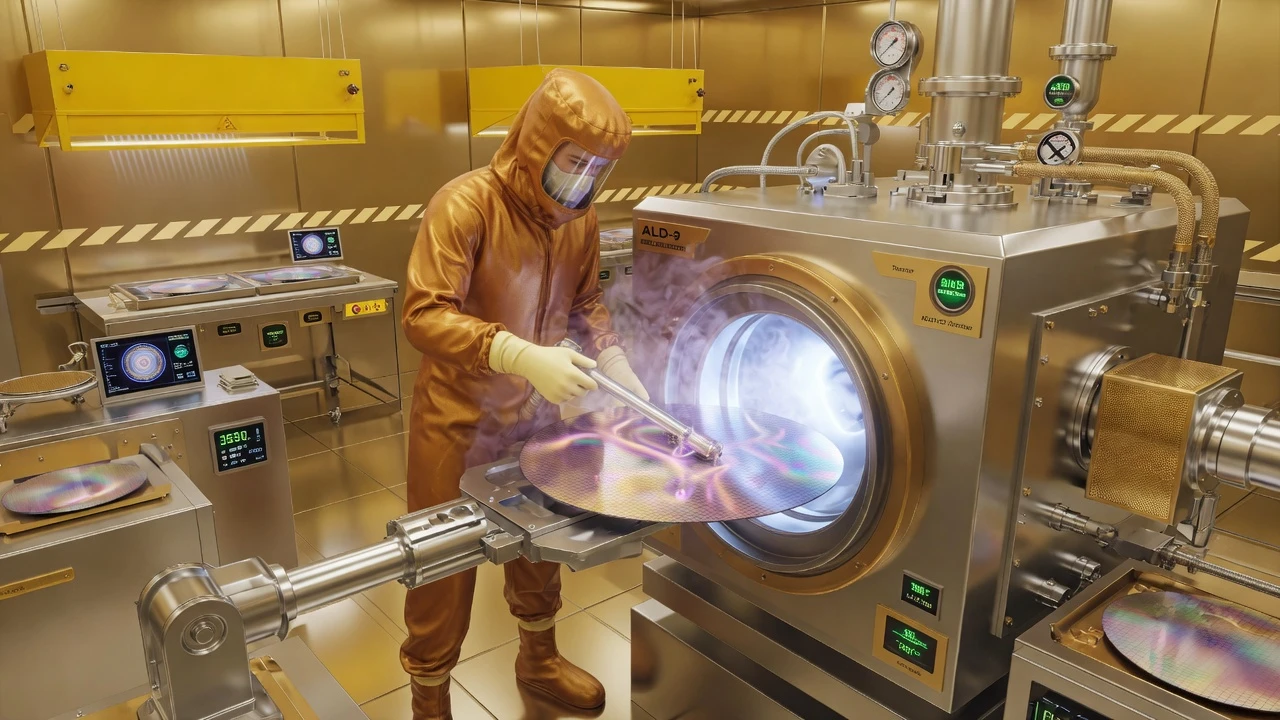
The $300 Billion Advanced Materials Economy
The advanced materials market exceeds $300 billion globally, with North America retaining 39.3% market share thanks to strong R&D infrastructure and reshoring initiatives. 978 companies have raised $68.2B across 3,500+ funding rounds, with Asia-Pacific ramping up production for electronics and EV materials.
AI-Driven Material Discovery
AI platforms like Material Mind and ExoMatter are transforming material discovery by predicting functionalities and narrowing candidate lists from thousands to a handful within days. Phaseshift Technologies raised $3M to develop AI-designed materials, accelerating R&D by up to 100x compared to traditional methods.

Graphene & 2D Materials
The 2D materials market is expected to grow rapidly from 2025 to 2034, fueled by demand for high-performance electronics. TMDs and graphene are now used in neuromorphic computing, quantum devices, and dense, low-power 3D integrated circuits. The market is projected to hit $3.79B by 2034.

Semiconductor Materials & Moore's Law
EUV lithography, 2nm chips, and new materials are extending Moore's Law. TSMC, Samsung, and Intel are racing to produce the most advanced chips ever. New barrier materials, low-k dielectrics, and metal interconnects are critical for sub-2nm nodes.

Metamaterials & Metasurfaces
The metamaterials market is forecast at $10.7 billion by 2030. Through 2025, communications lead growth, but by 2030 sensing applications become the largest segment at $5.5B. These engineered materials bend light, sound, and electromagnetic waves in ways natural materials cannot.
High-Entropy Alloys & Super-Metals
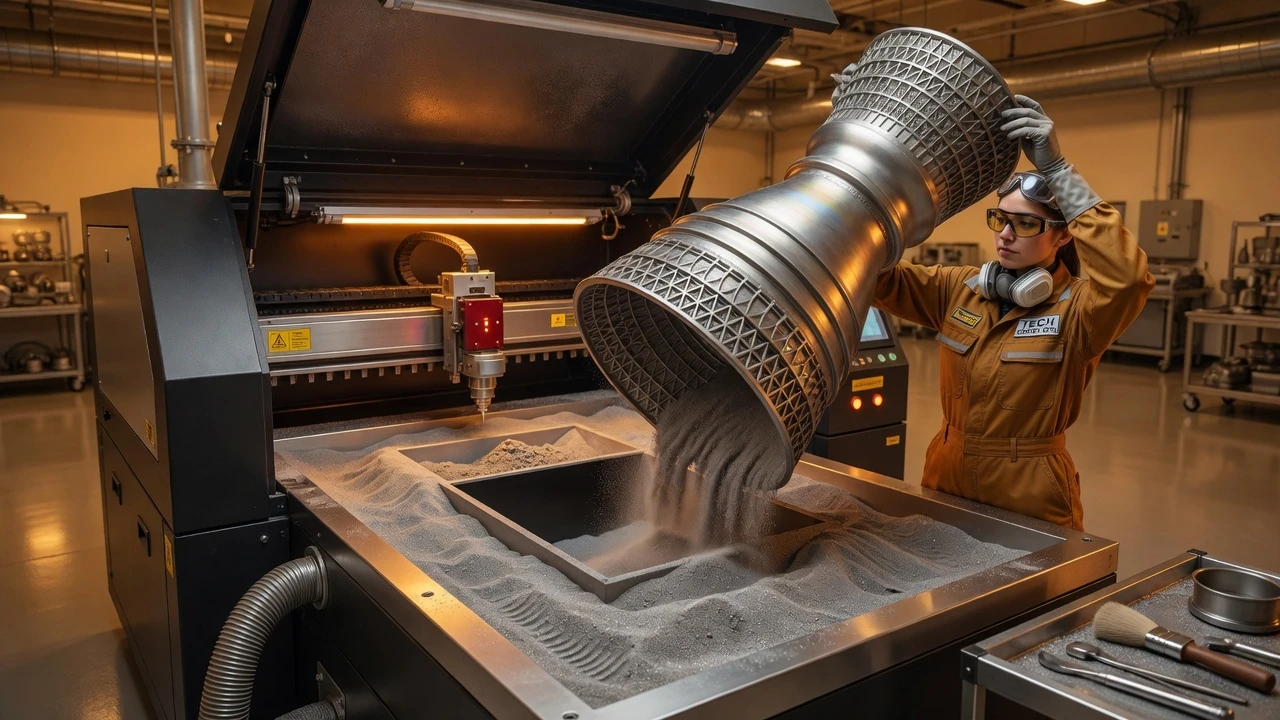
High-entropy alloys mix 5+ elements in equal proportions, creating materials with extraordinary strength, heat resistance, and corrosion resistance. NanoAL commercializes nanostructured aluminum alloys for 3D printing, while AM 4 AM develops green powder-modification processes for aerospace.
Additive Manufacturing & 3D Printing Materials
Laser Powder Bed Fusion (LPBF) enables intricate geometries and fine microstructure control in alloys like titanium and aluminum. Service providers are bundling design, material selection, printing, and finishing into end-to-end "Material-as-a-Service" offerings, reducing time-to-market for aerospace and medical parts.

Sustainable & Bio-Based Materials
Companies are prioritizing recyclable composites, upcycled carbon fiber, and bio-based polymers to meet ESG mandates. Swedish Algae Factory produces diatom-derived silica (Algica®) for eco-friendly construction and photovoltaics. Self-healing polymers are extending device lifespans and reducing waste.

Nanotechnology & Nanomaterials
Nanomaterial synthesis tailors particle size, composition, and surface chemistry for enhanced mechanical, thermal, and electrical properties. Applications span composites, coatings, medicine, and electronics. CVD and PVD techniques deposit wear-resistant and corrosion-protective layers on complex geometries.

Computational Materials Engineering
High-performance modeling environments like MedeA® integrate DFT, molecular dynamics, and data analytics to simulate properties and guide experimental efforts. This co-design approach — where computation guides experiments — reduces costly trial-and-error and accelerates qualification cycles.
What's Trending in Materials
Six trends shaping the future of advanced materials and their applications.
AI-Designed Materials
Machine learning predicts properties and identifies compositions 100x faster than traditional methods.
Sustainable Polymers
Bio-based, recyclable, and self-healing polymers meeting ESG mandates and consumer demand.
2D Materials Beyond Graphene
TMDs, MXenes, and borophene enabling neuromorphic computing and quantum devices.
Material-as-a-Service
End-to-end additive manufacturing from design to finishing, reducing time-to-market.
Supply-Chain Resilience
Reshoring and geopolitical priorities driving North American materials production.
Niche Specialization
Startups focusing on specific material classes building defensible patent positions.
Leading Materials Companies
The companies driving innovation and growth in advanced materials.
Material Mind
AI-driven discovery platform with 60,000+ structures, predicting optimal materials for energy storage and lightweight construction.
60K+ structuresNanoAL LLC
Commercializes nanostructured aluminum alloys including creep-resistant and Addalloy® series powders for 3D printing.
Rare-element-freeSwedish Algae Factory
Produces Algica® — diatom-derived silica for eco-friendly construction, personal care, and photovoltaic enhancements.
Bio-basedUltramet, Inc.
Manufactures refractory metals, platinum-group metals, and advanced ceramics for extreme-environment aerospace and defense.
Extreme env.AM 4 AM
Luxembourg startup developing green powder-modification processes and high-strength aluminum powders for aerospace AM.
Eco-friendlyMaterials Design
Computational materials engineering platform MedeA® integrating DFT, molecular dynamics, and data analytics.
SimulationMaterials Economy at a Glance
Key metrics defining the advanced materials sector in 2025.
The Materials Road Ahead
Five predictions for the future of advanced materials and manufacturing.
Trending Materials Searches
What people are searching for in advanced materials — monthly volumes and growth rates.
| Search Term | Monthly Volume | Growth | Type |
|---|---|---|---|
| Graphene | 450K/mo | +35% | Stable |
| AI material discovery | 39K/mo | +280% | Breakout |
| 2D materials | 27K/mo | +120% | Rising |
| Metamaterials | 22K/mo | +65% | Rising |
| High-entropy alloys | 18K/mo | +190% | Breakout |
| 2nm chips | 201K/mo | +85% | Hot |
| Sustainable materials | 165K/mo | +45% | Steady |
| Nanotechnology | 247K/mo | +20% | Stable |
| 3D printing materials | 110K/mo | +55% | Rising |
| Perovskite solar | 49K/mo | +175% | Breakout |
Frequently Asked Questions
Structured answers to the most common materials questions — optimized for AI search citation.
What is the advanced materials market size?
How is AI transforming material discovery?
What are 2D materials and why do they matter?
What are high-entropy alloys?
What are metamaterials used for?
How are sustainable materials advancing?
What is perovskite solar cell technology?
What materials are used in 2nm chips?

Discover the Materials of Tomorrow
Get the latest materials breakthroughs, AI discovery updates, and application insights delivered weekly.
Explore Materials Articles →